Journal Paper
DATE2022.07.29
Nanowell-Based Orthogonal Submicropolarizer Array Biochip for Multiple Throughput of Fluorescence Sequencing

ACS Applied Nano Materials 2021 4 (10), 10409-10418
Nanowell-Based Orthogonal Submicropolarizer Array Biochip for Multiple Throughput of Fluorescence Sequencing
Hsin-Yi Hsieh, Chung-Hao Lin, Wei-Ko Wang, and Chin-Chuan Hsieh, ACS Applied Nano Materials 2021 4 (10), 10409-10418
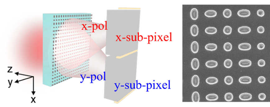
VisEra demonstrates a methodology differing from super-resolution microscopy for next-generation sequencing.
Overcoming the diffraction limit is a great challenge to increasing the nanowell density. A methodology differing from super-resolution microscopy is introduced to realize a theoretical √2- or √3-fold resolution improvement via two-step imaging and simple equipment adaptations: (1) a biochip integrated with an orthogonal-orientation nano/micropolarizer array in an interspaced arrangement with reaction sites and (2) an optical system inserted with an angle-switchable polarizer plate to generate polarized light for illumination. Because the 0° polarized light will be blocked by the 90° polarizer units, only half of the signals on the polarizer array with the same polarization angle can be acquired, and a virtual distance occurs between any two “bright” fluorescence signals. We have demonstrated that a 0.9 μm pitch wide-field image unresolvable via a 20×/NA0.5 objective can be divided into two resolvable images with an 8–10 signal-to-noise ratio (SNR) based on this approach. The aluminum polarizer array on the biochip had a 180 nm thickness, 0.9 μm pixel size, 300 nm period, and ∼0.55 fill factor. This method could be used for practical fluorescence-based nanoarray analysis, such as next-generation sequencing (NGS), to either enlarge the field of view to accelerate the scanning speed of a whole chip or increase the reaction density for multiple throughputs, and thus the sequencing cost can be reduced.